No products in the cart.
Abstract—We demonstrate a photonic platform that monolithically combines traditional crystalline Si waveguides and ultralow-loss Si₃N₄ waveguides (1.6dB/m) in a foundry-ready process. The material co-integration demonstrates high-density low loss delays and high-speed switch capabilities traditionally out of reach of Si₃N₄-only platforms, enabling high-performance analog photonics.
Index Terms—Silicon nitride, silicon photonics, optical device fabrication.
Ultra-low-loss (ULL) Si₃N₄ waveguides have gained attention as they support low propagation loss, high power handling, and enable non-linear optical functions. The resulting efficient optical delays and high quality factor (High Q) ring resonators empower advances including in RF signal processing, low noise synthesizers, spectroscopy, true time delays (TTDs), and finite impulse response (FIR) filters. Until now, however, ULL Si₃N₄ waveguides have not been monolithically integrated with classical Si photonics.
Silicon nitride waveguides have the capability to demonstrate optical losses below 0.5dB/m [1, 2], with thinner Si₃N₄ films having lower optical confinement and lower loss. However, this also results in very large bend radii (>1mm), limiting the usefulness of such platforms. Several platforms exist on this sliding scale between loss and bend radius, balancing this tradeoff to obtain moderate performance and reasonable device density [2]. The phase shifters are also limited to metallic heater-based thermo-optic phase shifters, which are slow and power-hungry compared to Si photonic thermo-optic and electro-optic phase shifters.
Traditional silicon photonics platforms often include Si₃N₄ waveguides, but due to thermal budget constraints in integration, their losses are orders of magnitude higher than standalone ULL Si₃N₄ platforms [1, 3], greatly limiting capabilities and applications.In contrast, GXC has built a photonic platform that uses the best aspects of both crystalline silicon and ULL silicon nitride, while overcoming their weaknesses. Here, Si₃N₄ waveguides are optimized for low-loss propagation and efficient facet coupling. Meanwhile, strip and ridge Si waveguides enable tight bends (<5μm radius) and doped Si heaters for phase shifting and switching. By implementing low-loss optical transitions between Si and Si₃N₄, each waveguide layer can be used adhoc in the system design. The fabrication is scalable, using only standard cleanroom processes and materials consistent with high volume CMOS foundries.
The fabrication begins with a commercially available silicon-on-insulator wafer with a 220nm device layer and a 3μm buried oxide (BOX). Following silicon strip and ridge waveguide formation, SiO2 is deposited by plasma-enhanced chemical vapor deposition (PECVD) to serve as the upper oxide cladding for the Si waveguides and the lower cladding for the Si₃N₄ waveguides. Following planarization, 150nm Si₃N₄ is deposited by low-pressure chemical vapor deposition (LPCVD), followed by lithography and etching to form the ULL waveguide layer. 150nm chosen as the Si₃N₄ thickness to provide sufficient optical confinement to avoid substrate absorption. A 4μm-thick SiO2 upper cladding is deposited and annealed at 1150◦C to reduce absorption and gradate the index between the core and cladding, further reducing loss [1].
Using a buffered oxide etch process, the thick upper cladding is selectively removed above the Si switch regions, locally using the Si₃N₄ layer as a selective etch stop with > 100:1 selectivity. Tuning of this etch process reduces slope angle and enables upcoming metallization to easily step into and out of these regions, aiding routing. A blanket dry etch then removes the Si₃N₄ from these regions. Trenches are patterned and etched into the middle cladding, and boron is implanted into the silicon. After RTA activation, 500nm PECVD SiO2 is deposited, patterned, and etched to open contacts to the implanted regions. Finally, Al(1%Si) is sputtered, patterned, etched, and sintered to from ohmic contacts to the p+ implant regions, realizing the completed platform shown in Fig. 1a.
This split-flow integration differs from traditional approaches in that the Si is formed structurally, but all implants and metallization processes are delayed until after the high temperature Si₃N₄ processes. Although not demonstrated here, the platform is also compatible with electro-optic modulators and p-i-n phase shifters, as once the upper cladding is selectively removed, multiple lithography and implant cycles can be implemented on the Si waveguides.
A. Optical Behavior
Si₃N₄ waveguides demonstrate optical losses of 1.6dB/m, as measured by optical backscatter reflectometry (OBR) as in [1]. Si ridge and strip losses are 0.88dB/cm and 5.4dB/cm respectively, which are similar to traditional silicon photonic platforms [3]. To our knowledge the ultra-low loss of the Si₃N₄ waveguide is the lowest
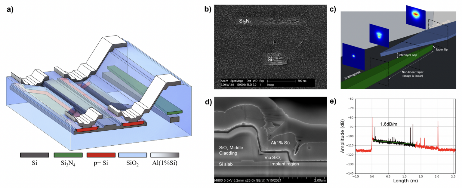
Fig. 1. a) Si/Si₃N₄ platform schematic, b) Interlayer coupler cross-section, c) Interlayer coupler schematic illustrating modal transition, d) Si implant contact region and metallization, e) OBR trace to determine Si₃N₄ propagation loss.
respectively, which are similar to traditional silicon photonic platforms [3]. To our knowledge the ultra-low loss of the Si₃N₄ waveguide is the lowest reported for a vertically stacked waveguide layer.
Si to Si₃N₄ optical interlayer couplers are formed throughnon-linear inverted adiabatic tapers, as shown in Fig. 1ac. Current results demonstrate transition losses of 0.23dB, but simulations suggest further optimization should drive this down to 0.02dB.
B. Switch Behavior
Mach-Zehnder Interferometers (MZIs) are formed as thermo-optic switches, with p+ resistors running parallel to the optical path on both sides of the Si ridge waveguides. By integrating these heaters directly into the Si material, high thermal efficiency is maintained. As a result, a π phase shift can be achieved with just 55mW, with rise and fall times of 10μsec and 15μsec respectively. By using thermo-optic phase shifters, MZI arm mismatch is minimized, leading to extinction ratios greater than 43dB.
In this platform, delays are formed through a unique serpentine structure rather than traditional in-out spirals by migrating all optical bends to the Si waveguide layer. This design capability enables the use of straight-path multi-modal (MM) Si₃N₄ waveguides, as they offer lower loss than single-mode (SM) waveguides (8dB/m). These dense serpentine delays consist of MM Si₃N₄, MM to SM converters, interlayer (IL) couplers, and Si “U-turns” as shown in Fig. 2. Due to the low loss interlayer couplers and short Si waveguide turns, the net delay insertion loss is lower than single-mode (SM) Si₃N₄-only delays. The resulting layout for a 0.7ns delay improves density by a factor of 5, and achieves a net propagation loss of 3.1dB/m. Integrated SM and hybrid-MM ring resonators demonstrate intrinsic Q-factors > 3.4M and 13M respectively, enabling wavelength filtering and nonlinear optics.
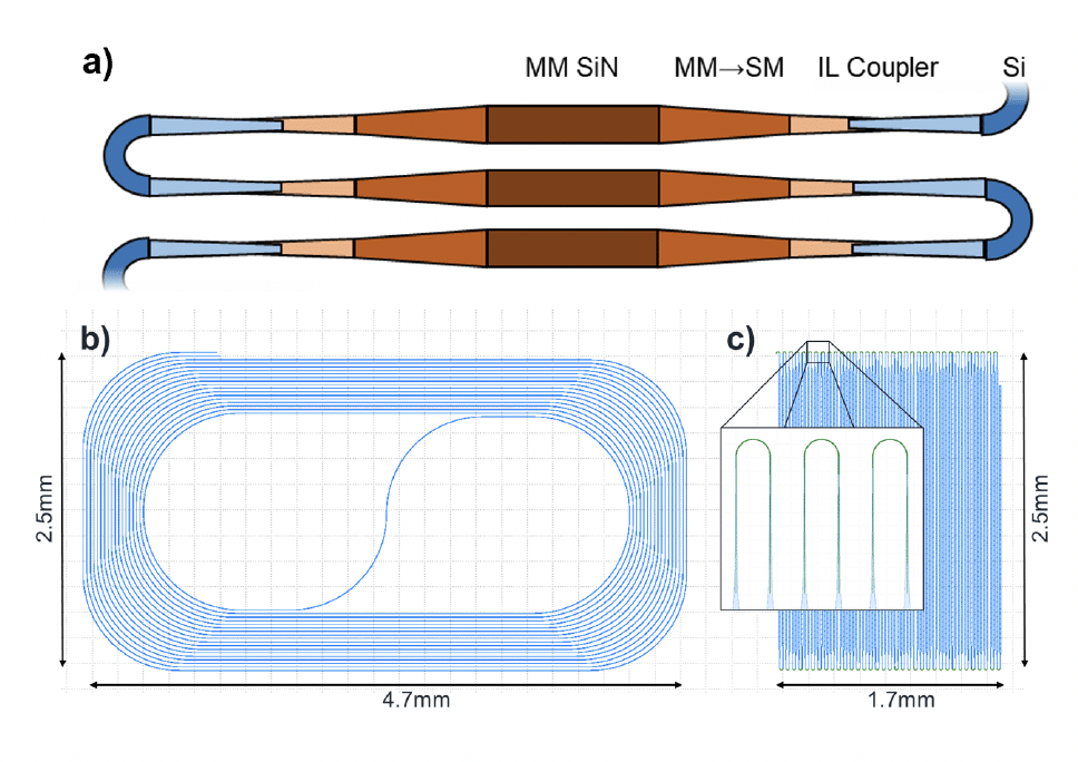
Fig. 2. a) Multi-element serpentine delay schematic, b) 0.7ns In-out delay spiral design on Si₃N₄-only platforms, c) Ultra-dense serpentine delay using this Si₃N₄ / Si platform.
We have demonstrated a photonic platform that monolithically integrates crystalline silicon with high-performance ULL Si₃N₄. This platform demonstrates the best of both material platforms – low propagation losses, high optical density, low power and fast switching – all in a foundry-compatible process. The platform enables many applications in digital and analog photonics, with clear design wins for TTDs and FIR filters.
REFERENCES
[1] J. Bauters, M. Heck, D. John, J. Barton, C. Bruinink, A. Leinse, et al, ”Planar waveguides with less than 0.1 dB/m propagation loss fabricated with wafer bonding,” Opt. Express vol. 19, 24090, 2011.
[2] D. Blumenthal, R Heideman, D. Geuzebroek, A. Leinse, and C. Roelofzen, ”Silicon Nitride in Silicon Photonics,” Proc of IEEE, vol. 106, Dec. 2018.
[3] N. Fahrenkopf, C. McDonough, G. Leake, Z. Su, E. Timurdogan, and D. Coolbaugh, ”The AIM Photonics MPW: A Highly Accessible Cutting Edge Technology for Rapid Prototyping of Photonic Integrated Circuits,” IEEE J. Sel. Top. Quantum Electron., vol. 25, Sep. 2019.